Angle Resolved Photoemission Spectroscopy
Introduction
The electronic band structure of a material constitutes the macroscopic basis of its physical properties; whether a solid is insulating, semiconducting, metallic, or superconducting, or if the material is transparent, or shows a distinct color, is determined by its electronic structure. The classical properties, like thermal conductivity, heat capacity etc. are determined by the electronic structure too. A detailed understanding of the electronic structure through microscopic investigations, along with theoretical analysis, is necessary in understanding and engineering new materials allowing for tunable control of their properties. The electronic states in a material is described by energy, momentum, and spin of the electrons.
Photoemission spectroscopy
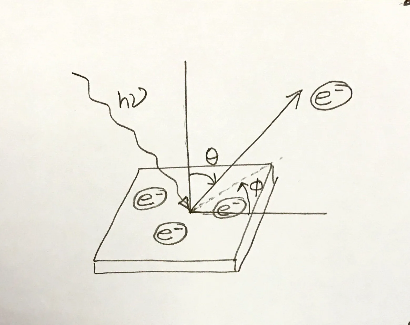
Photoemission spectroscopy is the most powerful, and the only tool available to directly probe the electronic structure of a material. Photoemission spectroscopy is based on the principle of photo-electric effect, in which the sample under investigation is irradiated with a beam of photon (laboratory discharge lamp or x-ray source or synchrotron light sources). If the energy of the incident photon is large enough for the electron to overcome its binding energy and the work function of the material, an electron is emitted from the material, and can be detected by an electron spectrometer. The electron spectrometer records the kinetic energy of such electrons detected in a particular angle. The angular information is directly related to the momentum of the electron while inside the material. This in tern, let us learn about the full electronic bands inside the material.

Figure: Schematic of the photoemission process. The density of states of outgoing electrons is proportional to that of the material. This schematic is taken from the Hufner's book.
Let us consider a material which has the above electronic structure: it has two core levels, and valence band near the Fermi energy. Now, if we measure the intensity distribution of photo emitted electrons as a function of electronic kinetic energy, we would see something like shown in above figure. It is straight forward that the photoemission intensity is proportional the density of electronic states of the material, however, the spectra is broadened due to the finite resolution of the experimental technique.
Before the photon is absorbed by the electron, photon may travel a finite distance inside the material. After the photon is absorbed by the electron, the electron can travel in all direction, however we can detect only the electrons that are coming out of the surface. Also, the mean free path of electron inside a solid is very small. It depends on the kinetic energy of the electron. For UV photons, the typical mean free path is of the order of few angstrom. That is why photoemission spectroscopy in the UV range is extremely surface sensitive.
Now, the most important question is: what information can we obtain about the material by analyzing the energy and emission angle of the photo-emitted electrons. In every physical process, the total energy and momentum of the whole system is conserved. From the energy conservation, we can determine the binding energy of the electronic state from where the electron is photo-excited. And from the momentum conservation, we can determine the momentum vector of the electronic state. Therefore, we can effectively map the bandstructure of a material by ARPES.
This single particle assumption of the photoemission process is simplified. In a real material, the electrons are not independent free particles. They are subject to many-body interaction. Therefore, interpreting the band structure from the observed photoemission spectra is not often trivial. We need some theoretical modelling and understanding of the system.
Resources
- Photoelectron Spectroscopy : Principles and Applications by Stefan Hüfner
- Angle-Resolved Photo Emission Spectroscopy entry on Wikipedia (PDF)